Google Taps AMD to Design Its Next-Gen TPU
The quietest power shift in AI hardware yet
For nine generations, Google designed its TPUs the same way: custom accelerator silicon, built with Broadcom, scaled to planet-sized clusters. The CPUs were always separate -- racked alongside the TPU pods, handling orchestration while the tensor cores did the heavy math. That division of labor is cracking.
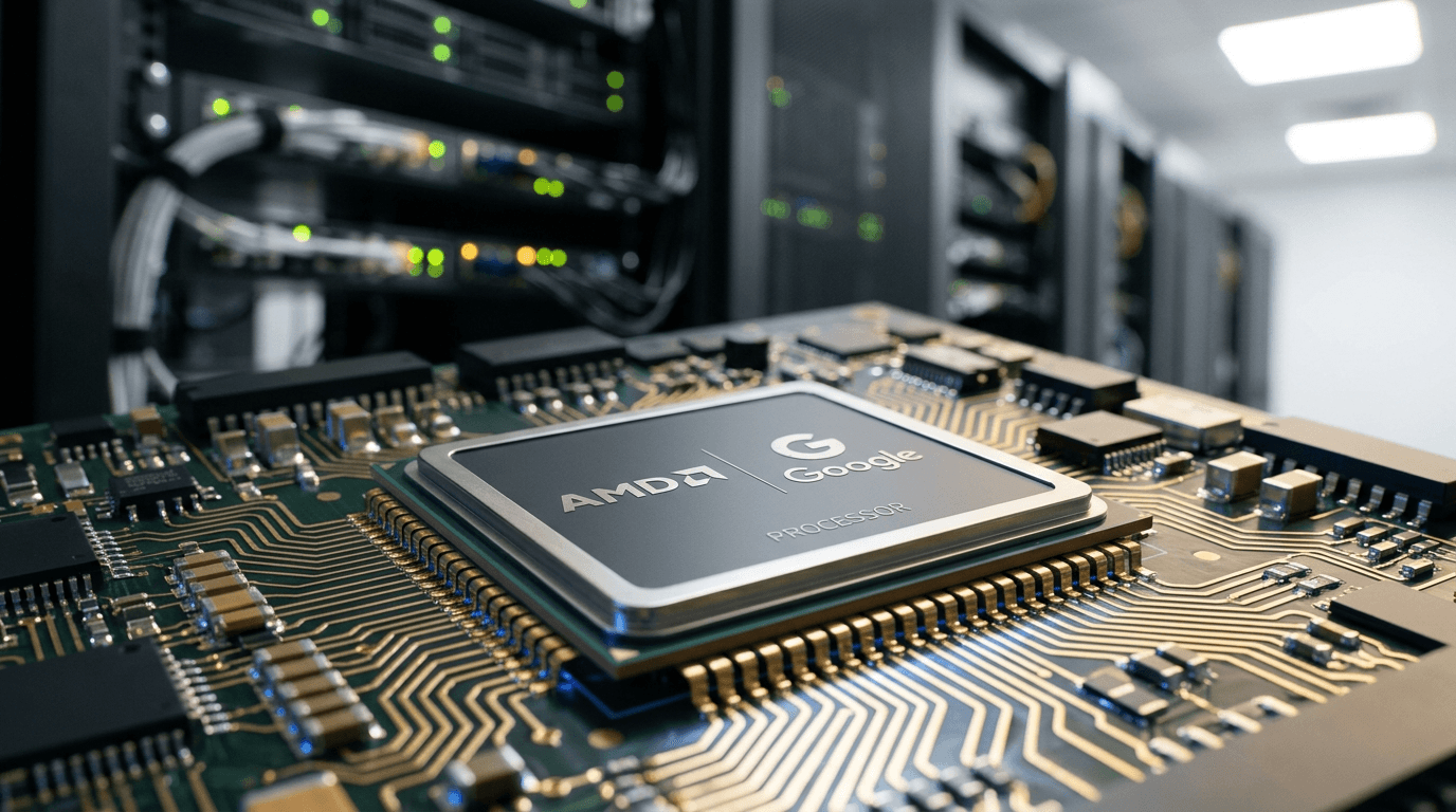
A note from SemiAnalysis, cited by Tom's Hardware, reports that Google is working with AMD on a v10 generation TPU. Not for the usual accelerator math -- but for what comes after it. The new chip would integrate CPU cores directly on the TPU package, purpose-built for reinforcement learning and agentic AI workloads that demand something traditional accelerators weren't designed to deliver.
Why a TPU suddenly needs CPU cores
The shift is grounded in a measurable trend. Google's TPU 8i systems, launched earlier this year, already use one Axion CPU for every two TPUs. The previous generation (TPU v7) ran at one CPU per four TPUs. SemiAnalysis reports that some workloads are pushing toward a 1:1 ratio of CPUs to accelerators.
Reinforcement learning is the driving factor. Training an LLM is overwhelmingly accelerator-heavy -- dense matrix multiplications that TPUs and GPUs handle efficiently. But reinforcement learning for reasoning models and agentic systems involves loops of trial, evaluation, and adjustment. Each iteration requires general-purpose compute to simulate environments, update policies, and manage state between inference calls. That compute is CPU work, not tensor work, and stuffing it through a separate server adds latency and power overhead.
Google's solution: bring the CPU onto the accelerator package. AMD's Instinct MI300A -- which packs x86 cores and accelerator chiplets into a single package -- provides a working template for this approach.
AMD's first real ASIC play
If the report is accurate, this would be AMD's first substantial involvement in a custom AI ASIC project. Despite having a custom silicon team, AMD has never been tapped by a hyperscaler to co-design a purpose-built AI chip. The SemiAnalysis note emphasizes that AMD's appeal lies in three areas: CPU IP (AMD's x86 cores for on-package compute), advanced packaging know-how (including its SoIC technology demonstrated in the MI300A), and interconnects optimized for hybrid workloads.
The report, however, cautions that AMD is unlikely to design Google's standard TPU compute -- that remains Google's own architecture. The partnership appears focused on the CPU-integration layer: building the general-purpose side of what would be a hybrid chip, while Google's tensor cores handle the accelerator math.
What this says about AI's next phase
The conventional narrative around AI infrastructure is that the future belongs to maximally specialized accelerators -- bigger TPUs, faster GPUs, denser matrix engines. The Google-AMD story suggests a more nuanced picture: as AI moves from training monolithic models to running iterative, agentic systems at scale, the bottleneck may not be tensor FLOPS but the general-purpose compute wrapped around them.
Google's v10 TPU, if it materializes as described, would be the first major hyperscaler chip explicitly designed for this post-training reality. It acknowledges that reinforcement learning and agentic AI -- the same forces driving the industry's most ambitious roadmaps -- demand a different kind of silicon than the one that got us here.
The SemiAnalysis note is a client document and not publicly available. The Tom's Hardware report is linked below.
Sources
- Tom's Hardware: Google reportedly taps AMD to design next-generation TPU
- SemiAnalysis (via Tom's Hardware): Analyst note on Google TPU v10 and AMD collaboration
- Google Blog: We're launching two specialized TPUs for the agentic era (context on TPU 8 architecture shift)